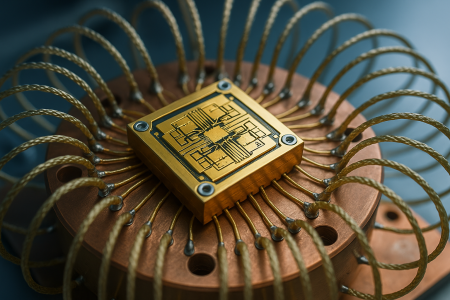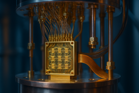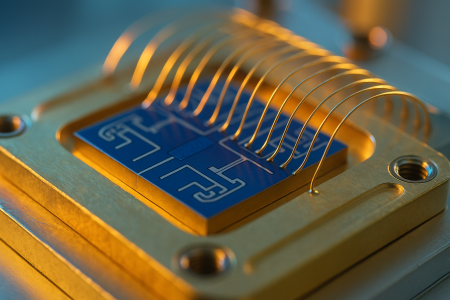

For years, a superconducting quantum processor lived on a single flat piece of silicon or sapphire. The qubits sat on the surface, and so did everything that talked to them: the resonators that read them out, the lines that delivered control pulses, the couplers that let neighbors interact. That works fine when you have a handful of qubits. It stops working when you want a hundred, then a thousand, all packed close together on the same plane. Something has to give, and what gives first is space.
The traffic jam on a flat chip
Picture a downtown grid where every building needs its own road, its own power line, and its own water main, all laid on the same street level. Add more buildings and the streets choke. A quantum chip faces the same problem. Each qubit needs a readout resonator, a drive line, and often a flux line to tune its frequency. Those structures take up area, and worse, they can accidentally couple to things they shouldn't. Signal lines crossing each other create stray capacitance and crosstalk, where a pulse meant for one qubit nudges another. On a single layer, wiring a large array without these collisions becomes a geometry puzzle with no clean solution.
The classical chip industry solved a version of this decades ago by going vertical. Modern processors stack many layers of metal interconnect above the transistors. Quantum engineers borrowed the instinct but not the exact method, because lossy dielectrics and dense metal stacks would poison the delicate coherence of a superconducting qubit. Their compromise is called flip-chip integration.
Two chips, face to face
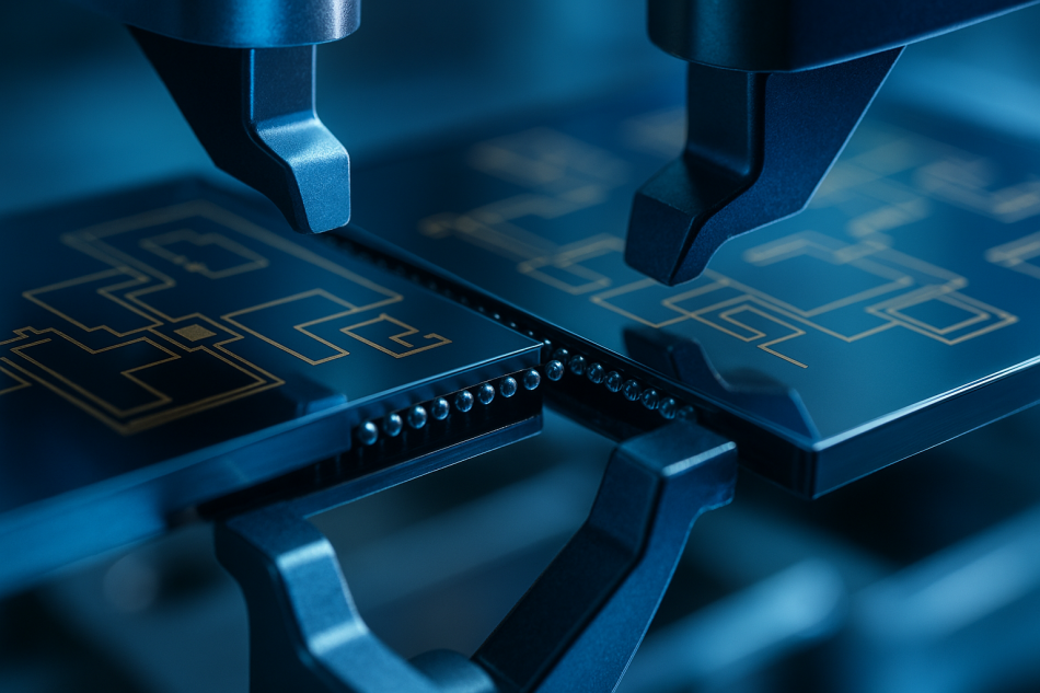
In a flip-chip design, the machine is split across two separate wafers. One chip carries the qubits and the couplers, the pieces that must stay as clean and low-loss as possible. The second chip carries the busy infrastructure: readout resonators, control wiring, and routing that would otherwise crowd the qubit plane. The two chips are then flipped so their patterned faces point at each other, and they are bonded together with a small gap in between, held by tiny pillars of superconducting metal, usually indium bumps.
The trick is that the qubits and their control lines now live on different floors of the same building. A signal can travel across the gap by capacitive or inductive coupling, or through a direct bump connection, without every wire fighting for the same surface. Suddenly there is room. Designers can place qubits in a two-dimensional array and route their signals up and out through the second chip, rather than trying to snake every line across a crowded plane to reach the edge.
Why the gap matters
The empty space between the two chips is not wasted. Keeping the lossy wiring physically separated from the qubits protects coherence, because the qubit's electromagnetic field spends less time in materials that dissipate energy. The size of that gap has to be controlled precisely, often to a few microns, because it sets the coupling strengths that the whole design depends on. Bond the chips a little too close or too far apart and the readout and control no longer behave as designed. This is why bump bonding, once a niche packaging step, has become a core competence for companies building large superconducting machines.
Several major efforts lean on this architecture. Google's processors use flip-chip bonding to separate qubits from their wiring, and IBM has described multi-layer and flip-chip approaches as part of how it plans to keep scaling qubit counts without drowning in crosstalk. The technique has quietly become one of the enabling steps that let chip sizes grow from dozens of qubits toward hundreds.
The catches
Stacking chips introduces new failure modes. Each indium bump is a mechanical and electrical joint that must survive being cooled to a few thousandths of a degree above absolute zero, where thermal contraction pulls on everything. A single bad bond can strand a qubit. Aligning two patterned wafers with micron precision, then bonding them without contaminating the surfaces, demands cleanroom discipline that not every lab has. And the more elaborate the packaging, the harder it becomes to diagnose which layer caused a problem when a device underperforms.
Still, the direction is clear. A flat chip has a hard ceiling on how much you can wire before the layout defeats you. Splitting the machine into a clean qubit floor and a busy service floor buys room to grow. It is not the whole answer to scaling, which also demands better cabling, colder amplifiers, and error correction. But it is one of the structural moves that turned the superconducting quantum processor from a single crowded tile into something with architecture.