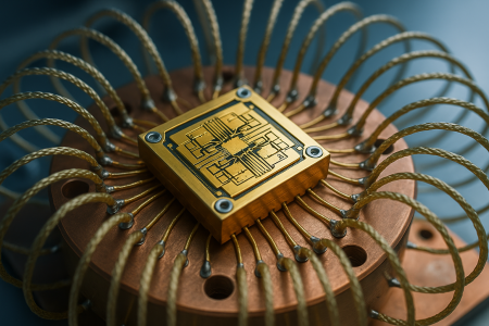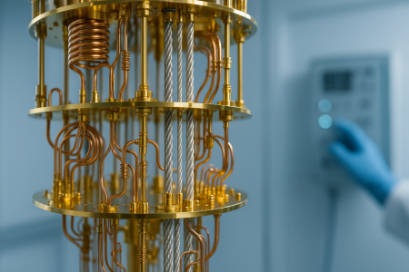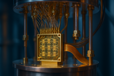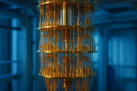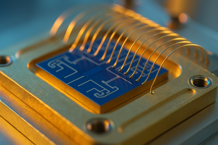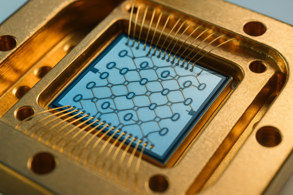

Look at a photograph of an IBM quantum processor and you will notice something odd about the pattern. The qubits are not packed into a tidy square grid the way pixels are on a screen. Instead they sit in a stretched honeycomb, with many of them touching only two neighbors. IBM calls this the heavy-hex lattice, and the sparseness is not an accident or a manufacturing compromise. It is a bet about what actually limits a superconducting quantum computer.
Connectivity is a double-edged sword
Every qubit that talks directly to another qubit is a convenience for the programmer. If two qubits share a physical coupling, you can entangle them with a single gate. If they do not, the compiler has to shuffle quantum information across intermediate qubits using SWAP operations, and each SWAP adds noise. So on paper, more connections are better. A densely connected chip runs shorter, shallower circuits.
The problem is that every connection is also a doorway for trouble. Superconducting qubits are electrical circuits, and putting them close together with strong couplings invites crosstalk: driving one qubit leaks energy into its neighbors, and two qubits with similar frequencies can accidentally exchange excitations. The more neighbors a qubit has, the more ways it can be disturbed, and the harder it becomes to find a set of operating frequencies where nothing collides. On a dense square grid where each qubit couples to four others, these frequency-collision constraints pile up fast, and manufacturing yield suffers because a single badly placed qubit frequency can spoil a whole neighborhood.
The honeycomb compromise
The heavy-hex layout is IBM's answer to that pressure. In it, most qubits have only two or three neighbors instead of four. The lower connectivity dramatically loosens the frequency-crowding problem: with fewer couplings per qubit, there is more room to space frequencies apart and avoid the collisions that kill performance. Crosstalk drops because each qubit simply has fewer companions to interfere with. The result is a chip that is easier to fabricate reliably and quieter to operate.
The word "heavy" refers to extra qubits sitting on the edges of the hexagons, between the corner qubits. Those bridging qubits do something clever in the context of error correction. IBM designed the lattice to suit a particular family of quantum error-correcting codes, where some qubits carry data and others act as measurement helpers, or ancillas. The heavy-hex geometry maps neatly onto codes that need each check qubit to touch only a couple of data qubits, which again keeps the wiring and the crosstalk manageable.
What it costs the programmer
Sparseness is not free. Because qubits far apart on the chip cannot interact directly, algorithms that assume all-to-all connectivity, common in the trapped-ion world, must be heavily rewritten to run on heavy-hex hardware. The compiler inserts SWAP chains to route information from one region of the chip to another, and those chains eat into the noise budget. A circuit that looks compact on paper can balloon once it is mapped onto the real connectivity graph. This is the same SWAP tax that haunts any limited-connectivity machine, and it is the price IBM decided was worth paying for cleaner physics.
The trade-off sharpens the contrast between hardware families. Trapped-ion and neutral-atom machines can often connect any qubit to any other, so they sidestep routing overhead entirely, but they pay elsewhere in speed or scaling difficulty. Superconducting chips are fast and fab-friendly, but they live and die by their two-dimensional layout. Heavy-hex is IBM's particular resolution of that constraint.
A design that shaped a roadmap
The heavy-hex lattice has been the connective tissue of IBM's processor line for years, from the earlier chips through the larger devices that stitch multiple dies together. As IBM moves toward error-corrected machines, it has begun exploring newer codes and coupling schemes that call for slightly denser or differently shaped connectivity, including longer-range couplers that reach across the chip. That evolution is telling. The honeycomb was the right answer for an era dominated by crosstalk and frequency collisions, but as those problems come under control, the optimal geometry shifts.
The lesson underneath the pattern is that a quantum chip's layout is never just cosmetics. Where you place the qubits, and how many neighbors each one gets, encodes a whole philosophy about which errors you fear most. IBM looked at its qubits, decided that crowding was the enemy, and gave each one a little breathing room.